
Crumbling the Memory Wall with High Bandwidth Flash (HBF)
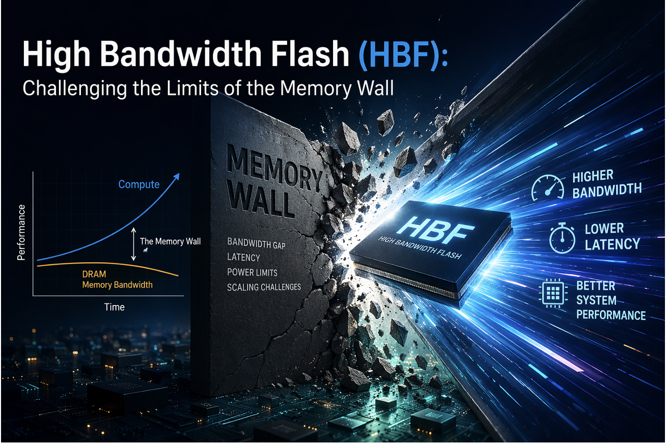
Much repeated, now well-acknowledged is the Memory Wall challenge. It might be a serious obstacle in the AI Infrastructure world; however, it gives the AI researchers and AI memory-focused companies a chance to get innovative. There is compute power lying waste and underutilized because of insufficient memory to tackle huge amounts of data involved in AI processing. In the initial rush, the hyperscalers and neoclouds tried getting around the memory crunch by adding more of GPUs. GPUs like Nvidia’s H100 and A100 have HBM chips placed immediately next to the GPU die on a single package using a silicon interposer. This proximity reduces data transfer latency and increases memory bandwidth, which is so crucial for heavy AI training/inference and high-performance computing. Just as a reminder, here’s a very simplified image of a GPU in the context of compute and memory.
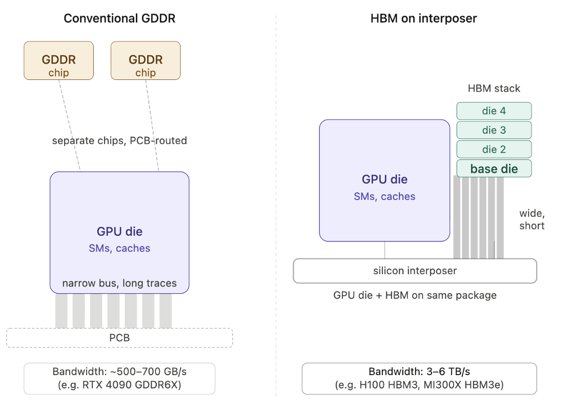
The image on the left shows a GPU with the GDDR chips. In this approach, separate memory chips sit on the PCB and connect to the GPU die via long traces with a relatively narrow bus. With HBM (the image on the right), the memory is stacked vertically in multiple dies (connected through tiny holes called through-silicon vias or TSVs), and the whole stack is placed right next to the GPU die on a shared silicon interposer — essentially a finely-wired slab of silicon acting as a high-density routing layer.
That’s good, but maybe not as good, as modern AI inference for LLMs with sequence lengths of up to 10 million tokens might require a huge amount of memory (up to terabytes of cache) for storing the KV (key-value) caches during inference.
Compute over-provisioning by adding more of GPUs, to get more of scarce memory is a wasteful and inefficient approach.
Let’s revisit some concepts around HBM.
A brief on HBM
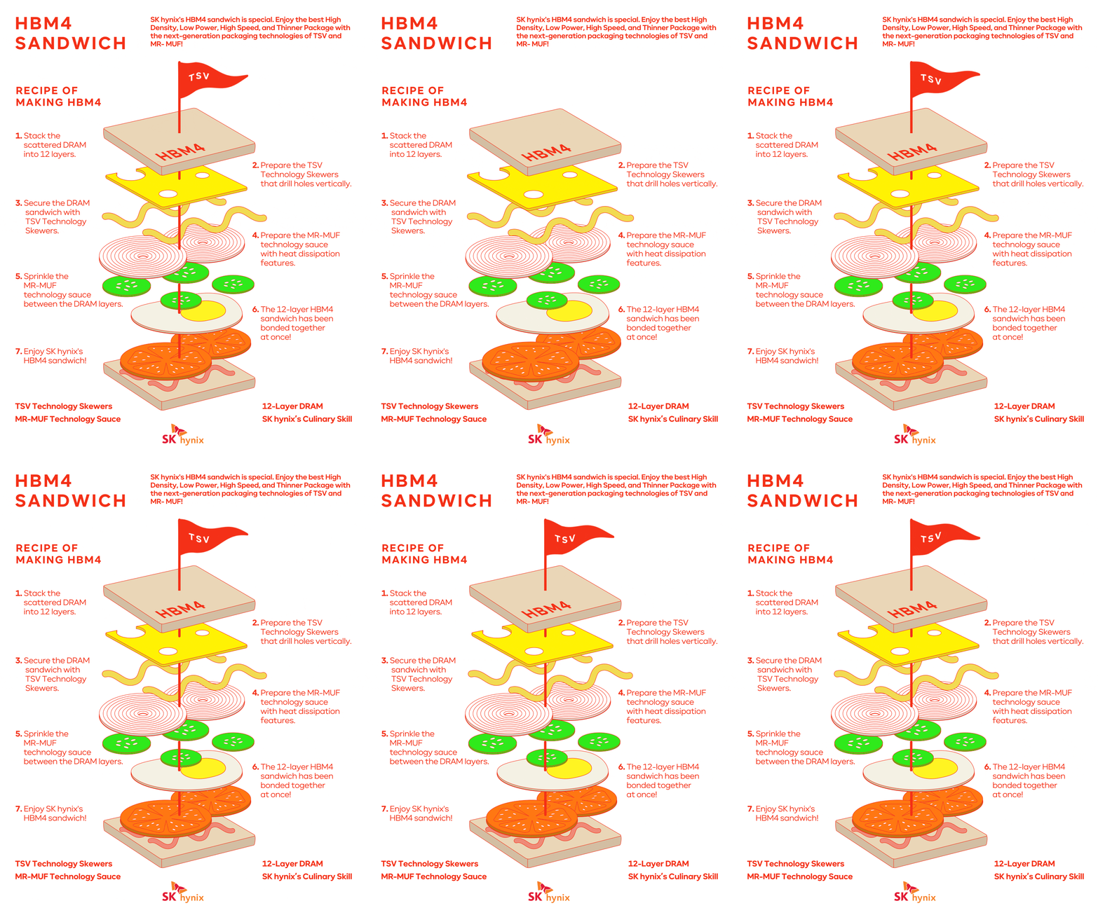
High Bandwidth Memory (HBM) is used in GPUs within AI accelerators today, as a vertically-stacked memory, which in particular contains many thin DRAM chips that are 30–50 µm thick, and, with the topmost die often being thicker. HBM commonly stacks 4, 8, or 12 dies together. In newer generations such as HBM4, the stack increases to 16 dies. These layers are stacked and secured to each other via TSVs. This creative graphic from SK Hynix on World Sandwich day explains it nicely.
Limitations of HBM
However, HBM has the following limitations:
Limited Capacity
High Cost
High power consumption
Thermal constraints
In the AI world, the memory capacity and bandwidth requirements are burgeoning. The “Father of HBM”, Professor Kim Joung-ho of the Korea Advanced Institute of Science and Technology (KAIST), says that 100 TB memory will be required in the upcoming AI interactions. When memory capacity hits the ceiling, it is generally the time to switch to storage, the persistent memory. Relying on NVMe over PCIe SSDs is not the answer because of PCIe bus latency.
Enters High Bandwidth Flash or HBF, which aims to serve as an intermediary layer between HBM and the slower NVMe SSDs. The base architectural concept remains similar to HBM. Supported by the Father of HBM, HBF is not a new storage medium—it is an architectural shift that combines 3D NAND flash memory with the advanced packaging and interconnection technologies pioneered by HBM. The goal is to provide high-capacity, low-cost flash memory with data transfer speeds approaching high-end memory.
Architecture of HBF
In HBF, instead of the DRAM layers, NAND Flash layers are used. The advantage of such an arrangement is that since Flash is easily and cheaply available, the hungry compute algorithms get plenty of storage.
Main HBF Use Case
Memory capacity and bandwidth bottlenecks can adversely impact the performance of large language models. Memory performance is a decisive factor in determining AI performance. Performance-wise NAND Flash is slower than DRAM but it can complement DRAM in HBM by supplying huge storage capacity. NAND Flash has the structure that it is composed of 100s of layers of NAND, and if you stack it ten times over, it can result in thousands of layers thereby providing huge capacities of storage. HBF could be positioned to complement HBM’s limited capacity by storing entire large AI models such as GPT-4 on the GPU. No need for access to SSDs or other local mass storage units, or even the internet.
In such a system HBM serves as a fast cache for temporary data processing, while HBF acts as the main memory holding massive AI models.
Given its write endurance limitations, HBF is best suited for read-intensive workloads—making it ideal for:
LLM inference with shared pre-computed KV caches
Read-heavy recommendation systems
For many AI inference tasks, the critical factor is high throughput at a feasible cost rather than the ultra-low latency that HBM or DRAM, for that reason, provides.
HBF Advantages
HBF has the advantages that it provides more memory capacity as compared to HBM. It is also less expensive to manufacture HBF as compared to HBM. The following list indicates all the advantages of HBF:
Up to 16× larger capacity than HBM
Similar bandwidth to HBM (~1.6 TB/s)
Lowest cost per bit of any high-bandwidth memory
Non-volatile (no power requirements for refresh)
HBF Ecosystem Players
It is believed that SK Hynix and Samsung are well-positioned to produce HBF in large quantities as both the companies are conversant with HBM, NAND Flash, and the packaging techniques used in creating HBM and hence, for HBF.
Another US player, SanDisk, prototyped and displayed the first of its HBF in the Future of Memory and Storage (FMS) 2025. They bagged the Most Innovative Technology award for that. Sandisk’s initial HBF prototypes leverage its proprietary BiCS NAND stacking and CBA wafer bonding technologies. While this might not be what’s the latest update on this matter, but SanDisk plans to get its first samples ready by end of 2026 and server scale samples by 2027.
Samsung has also initiated early design work in the field of HBF solutions.
Nvidia, the largest HBM consumer in the world and hence, the largest potential HBF customer has not commented on HBF yet.
A Note on Standardization
At FMS 2025, SK Hynix and SanDisk went on to join hands to sign a Memorandum of Understanding (MoU) to develop a comprehensive, technical, industry standard so that HBF could be commercialized and the customers have more options to choose from.
SK Hynix was instrumental in driving the adoption of HBM in the AI world. Together, the two companies are aligning to define the requirements and specs that will ensure that HBF scales both technically and commercially.
HBF Timeline
Sandisk shared its latest updates on the HBF development at the Flash Memory Summit held in 2025.
HBF is not in production, but first samples from Sandisk are expected in the second half of 2026, with first inferencing results likely in 2027.
Timelines
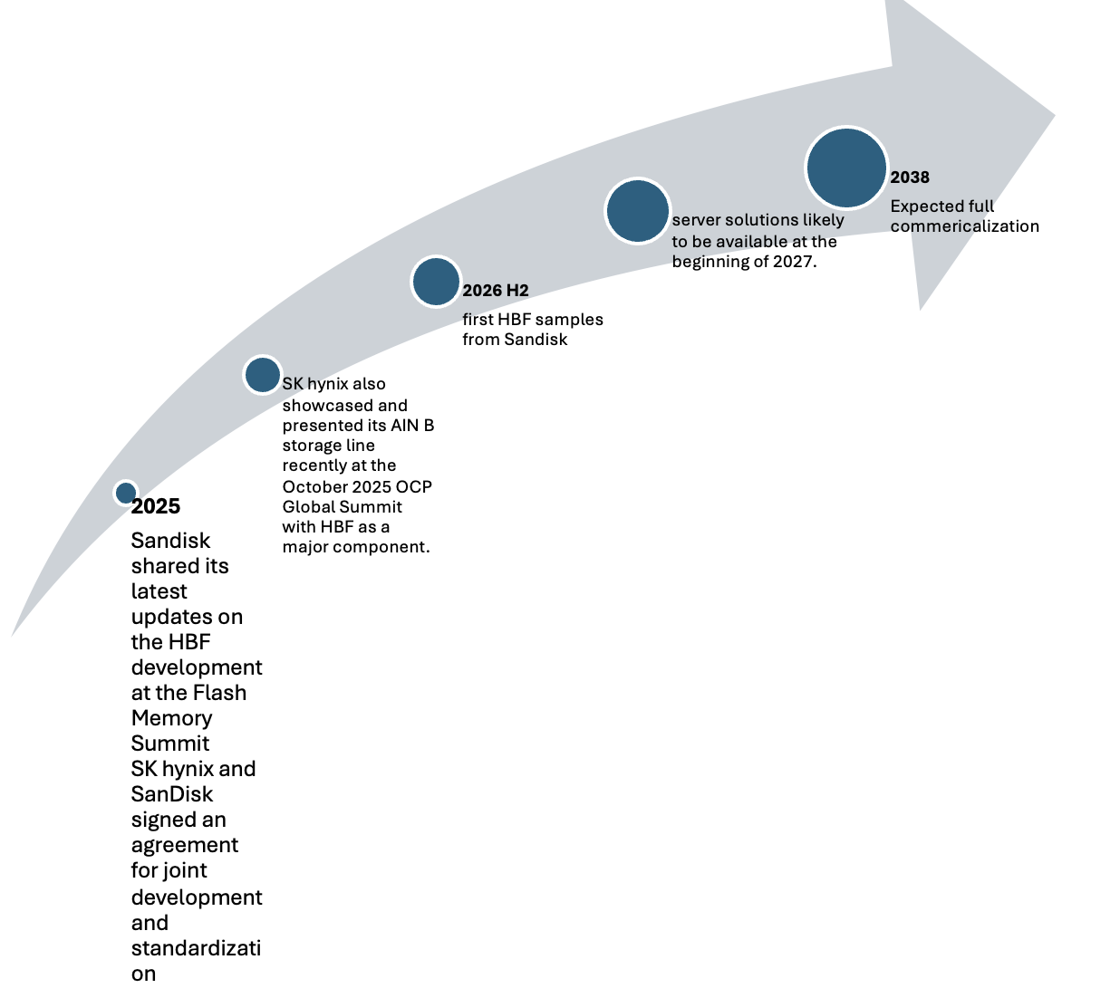
In August 2025, SK hynix and SanDisk signed an agreement for joint development and standardization.
SK hynix also showcased and presented its AIN B storage line recently at the October 2025 OCP Global Summit with HBF as a major component.
HBF memory samples should be ready in the second half of 2026, with server solutions likely to be available at the beginning of 2027.
The full commercialization is expected to take off by 2038.
HBF Specs
SanDisk's first-generation HBF product delivers impressive specifications:
Read Bandwidth: 1.6 TB/s
Density: 256 Gb per die
Total Capacity: 512 GB per 16-die stack
Capacity Advantage: 8–16× greater than HBM
Performance: Within 2.2% of unlimited-capacity HBM for inference workloads
Form Factor: Matches the physical footprint, power profile, and stack height of HBM4
According to sources, HBF acts as a supporting layer for large-scale data storage and efficient transfer. It delivers about 80 to 90 percent of HBM’s speed, but with 8 to 16 times the capacity and roughly 40 percent less power consumption. For large AI training and inference servers, it is widely described as a “mid-tier memory” that can relieve HBM bottlenecks.
HBF cannot replace HBM, but it does share the same electrical interface, so will only require minor protocol adjustments, according to Sandisk.
The H³ Architecture: HBM + HBF Hybrid
SK Hynix has proposed an innovative architecture called H³ that places both HBM and HBF on a single interposer connected to the GPU. This hybrid approach leverages the strengths of both technologies. Here’s the link to the IEEE paper describing this architecture.
HBF Limitations
The following are the limitations of HBF:
Higher latency (as compared to HBM)
Limited write endurance. NAND has a finite lifespan that can tolerate only a certain number of writes
Higher power consumption
Besides, there can be engineering challenges to put together multiple layers of NAND dies; each NAND die itself composed of multiple layers.
New Memory Hierarchy
As AI models continue scaling, the memory hierarchy will likely evolve from a two-tier system (HBM + SSD) to a three-tier architecture (HBM + HBF + SSD), with each tier optimized for specific access patterns.
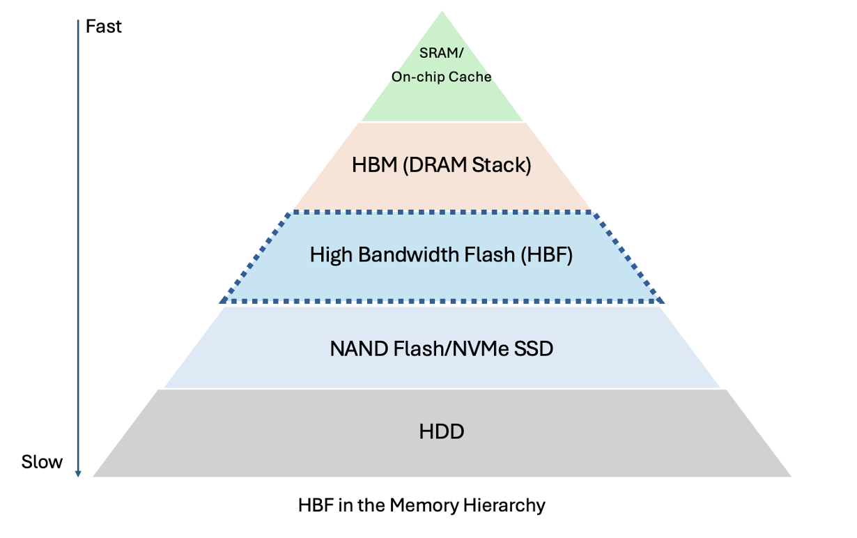
DRAM is fast but expensive and capacity-limited, while NAND flash is cheap and dense but too slow.
NAND-based HBF promises an alternative; not just as storage, but as a new memory tier. NAND flash is a denser memory technology that can supposedly provide 8-16 times more memory in the same footprint as HBM. It is, however, not without downsides. (as detailed above)
